When you read the data sheet correctly you can see, that the distance between the pins is different for a AA and AAA battery holder. That`s why I was asking if somebody can recommend a holder that fits.
This is an atmega328p based board for battery based sensors. Design was done in CADSoft Eagle 7.3 (free light version). Actual sensors are added via the extension pins. The board was designed to be fitted with a battery holder.
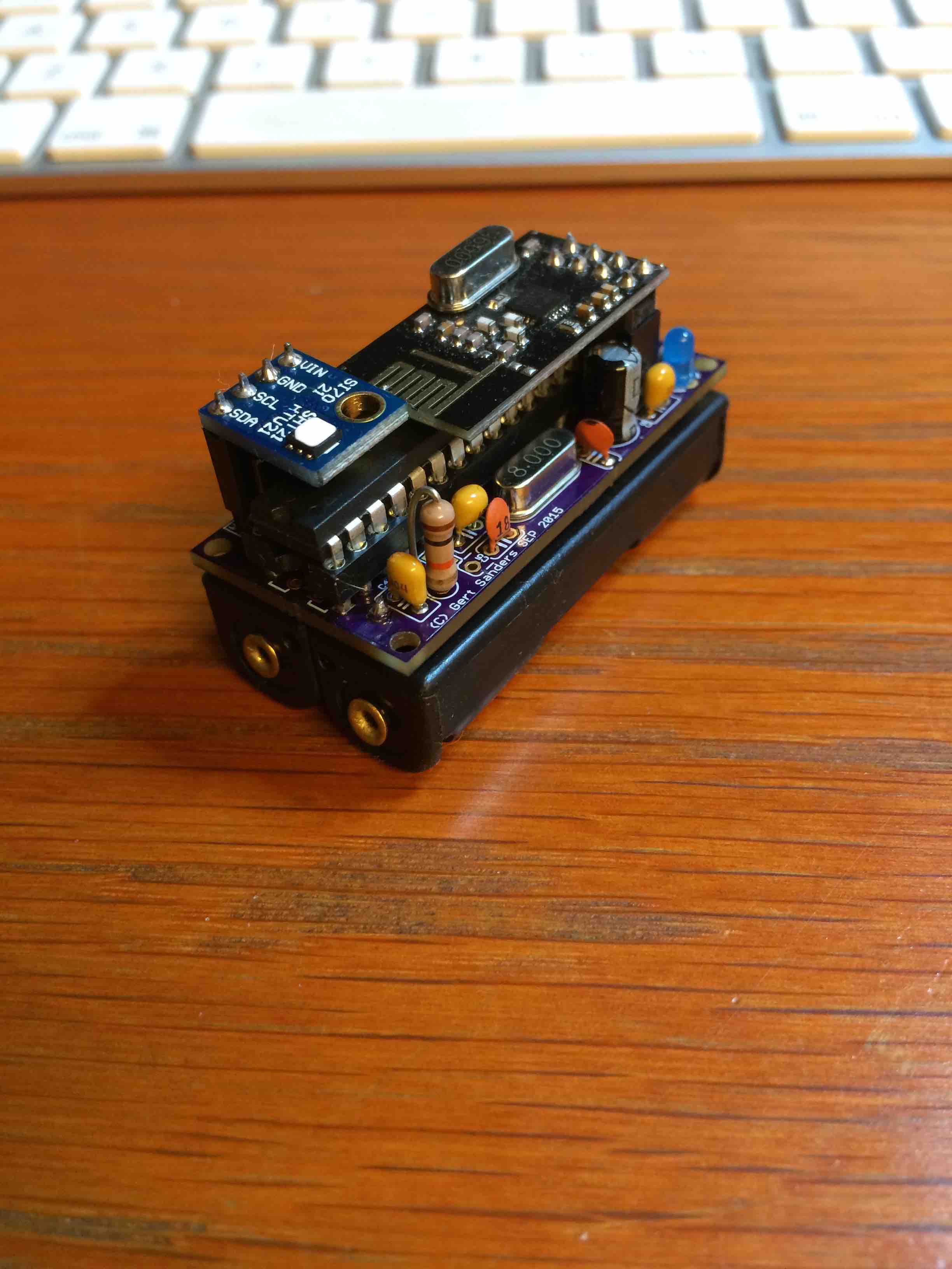
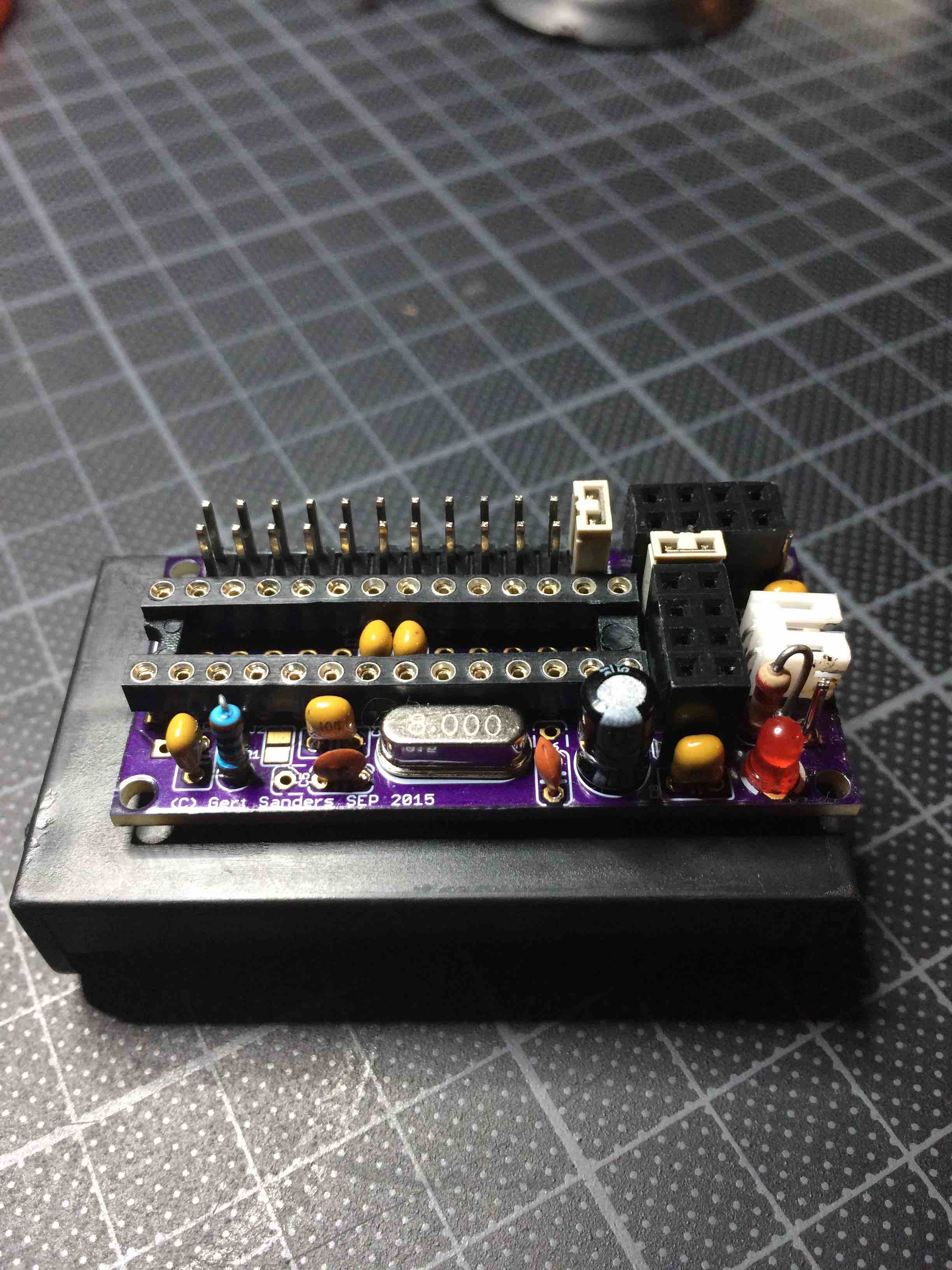
At the same time it should also allow connection with an expansion board which holds (in it's first version) a 3V3 regulator and some screw terminals.
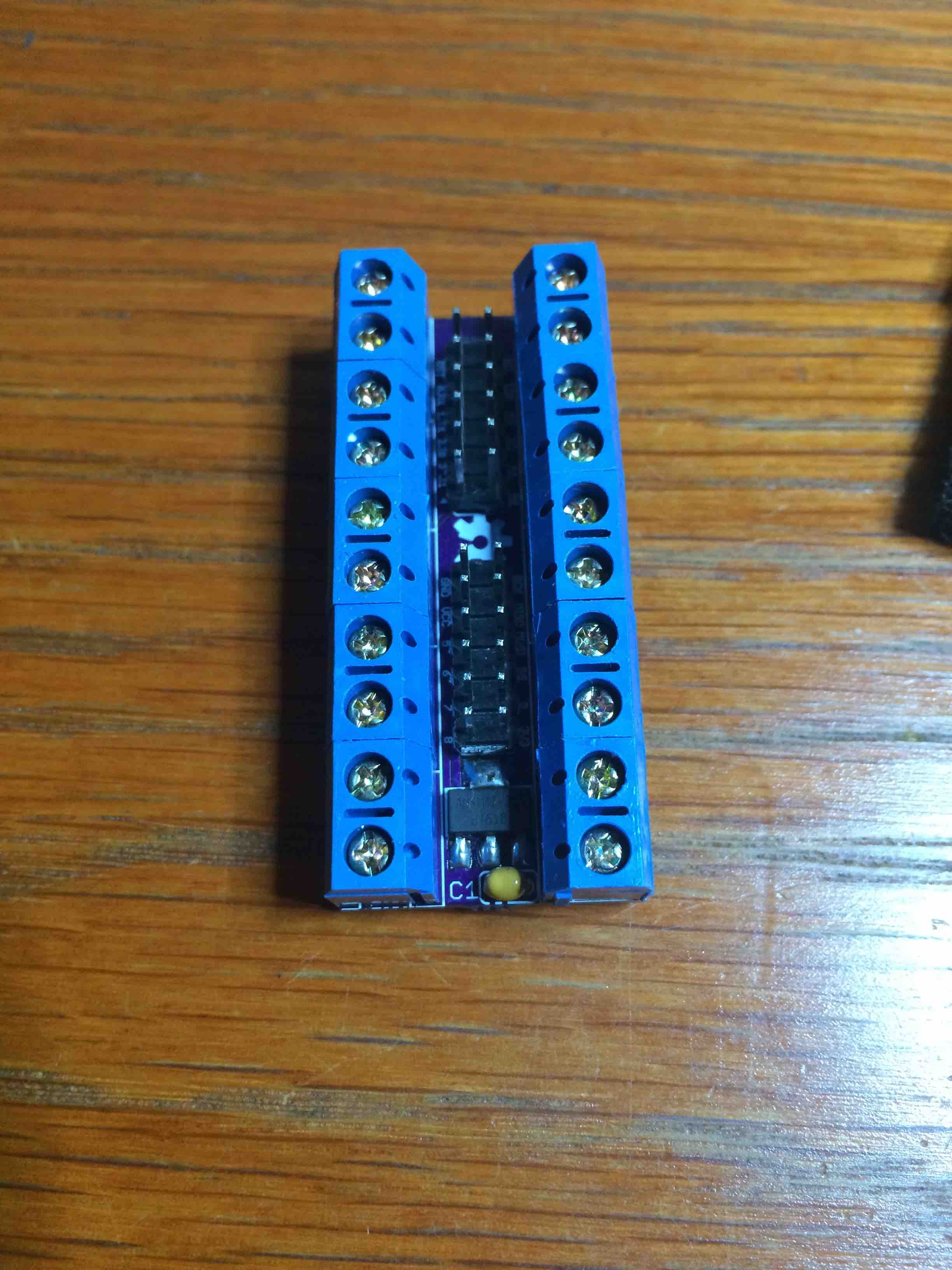
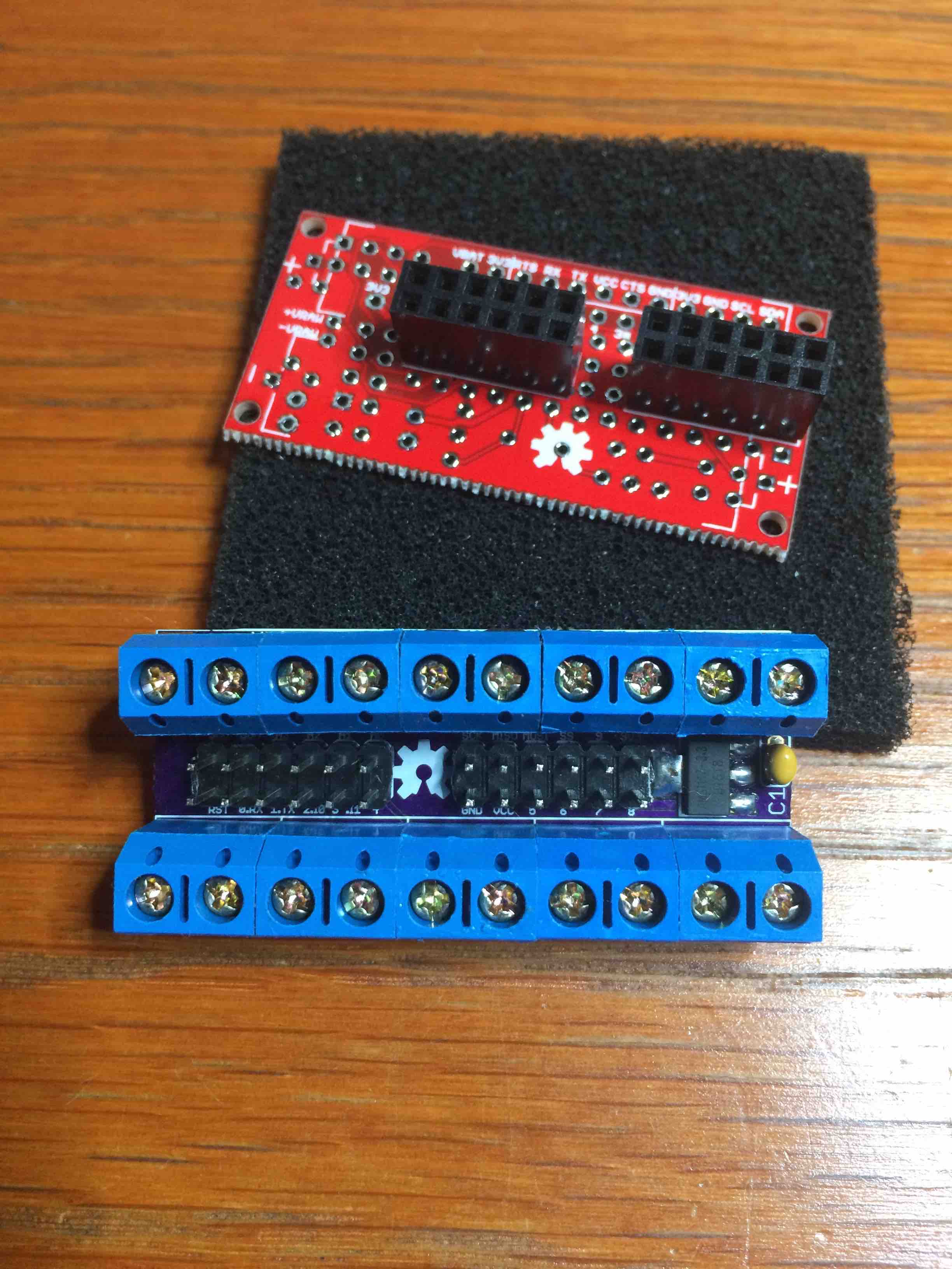
You need to power the node via an external power source (max 5VDC) if you plan to use the companion board. For this a JST connector can be fitted on the node board. The companion board below was originally meant for the first version of the battery based node. So there is a slight offset.
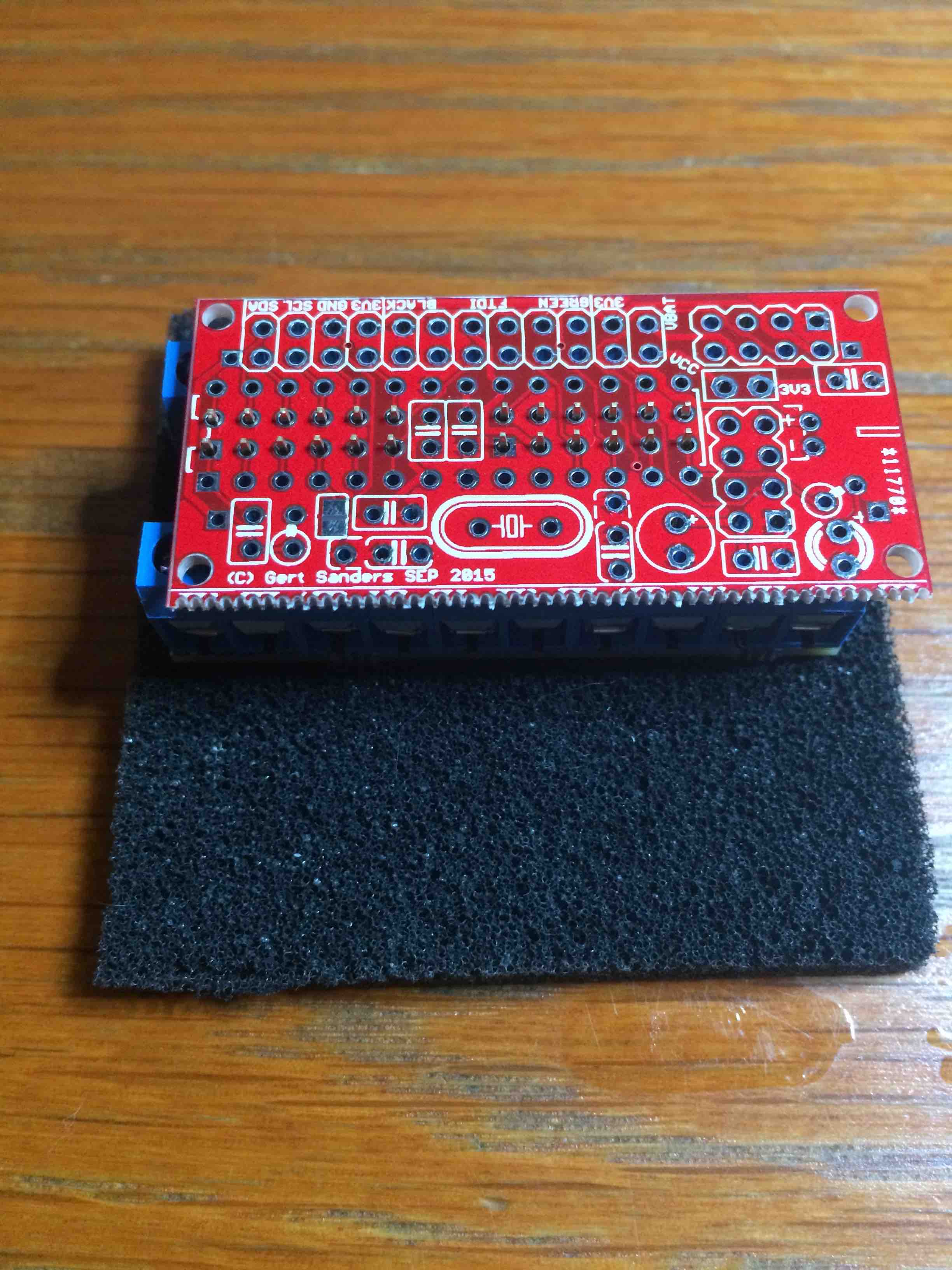
The layout of the extension connector is as follows:
ADC3      1   2  SDA
ADC2      3   4  SCL
ADC1      5   6  GND
ADC0      7   8  3V3
D2(INT0)  9  10  GND
D3(INT1) 11  12  no connection
D4       13  14  VCC
D5       15  16  TX
D6       17  18  RX
D7       19  20  RTS (RESET)
VRAW     21  22  3V3
VCC      23  24  VBAT
You can see the connection names on the silk screen on the bottom of the node board.
Powering options
If powered by two AA or AAA batteries, the circuits VCC and 3V3 should be connected. This is done by shorting jumper "J1".
The "JST" connector is connected to the VRAW circuit and to GND circuit. If the voltage on the VRAW circuit is within the limits of the NRF24L01+ (maximum 3.6V), then you can interconnect VRAW-VCC-3V3 If VRAW is e.g. 5V, then you can connect VRAW with VCC (as the atmega328p can handle 5V). But you should provide a 3V3 via the extension connector or via the companion board. There is no 3V3 regulator on the node board. You could use the LE33A directly on the node board and thus interconnect VCC-GND-3V3. This should give 3V3 but it is not tested, requires some slight hacking any feedback if this works would be nice. I'm lazy, I will rather design a new board then hack an existing one.
So I provide my 5V powered nodes with 3V3 via the companion board.
IC1 on this companion board is a AMS1117. C1 is a ceramic 100nF capacitor. The rest are headers and screw terminals.
If there is enough demand to add 3V3 regulation, a next version of the node board will have voltage regulation for the radio, there is just enough space for that.
This board allows the radio to be mounted in 2 ways. First one along the long axis of the board, second along the short axis of the board, whereby the antenna part of the nrf24l01+ is protruding from the outline of the board. The question is: do we need two possibilities ?
I find that in most of my boards I do not need the header to mount the radio with protruding antenna. I would like some feedback on that too.
Links to manufacturers to make the PCB:
The node board
https://oshpark.com/shared_projects/unP8BmuI (single boards)
http://dirtypcbs.com/view.php?share=11770&accesskey=5f9f38337641290cf017475f1b91ff81 (panelised version)
The companion board
