ok, thanks for reminder.
MySMotherboard
Motherboard for MySensors nodes
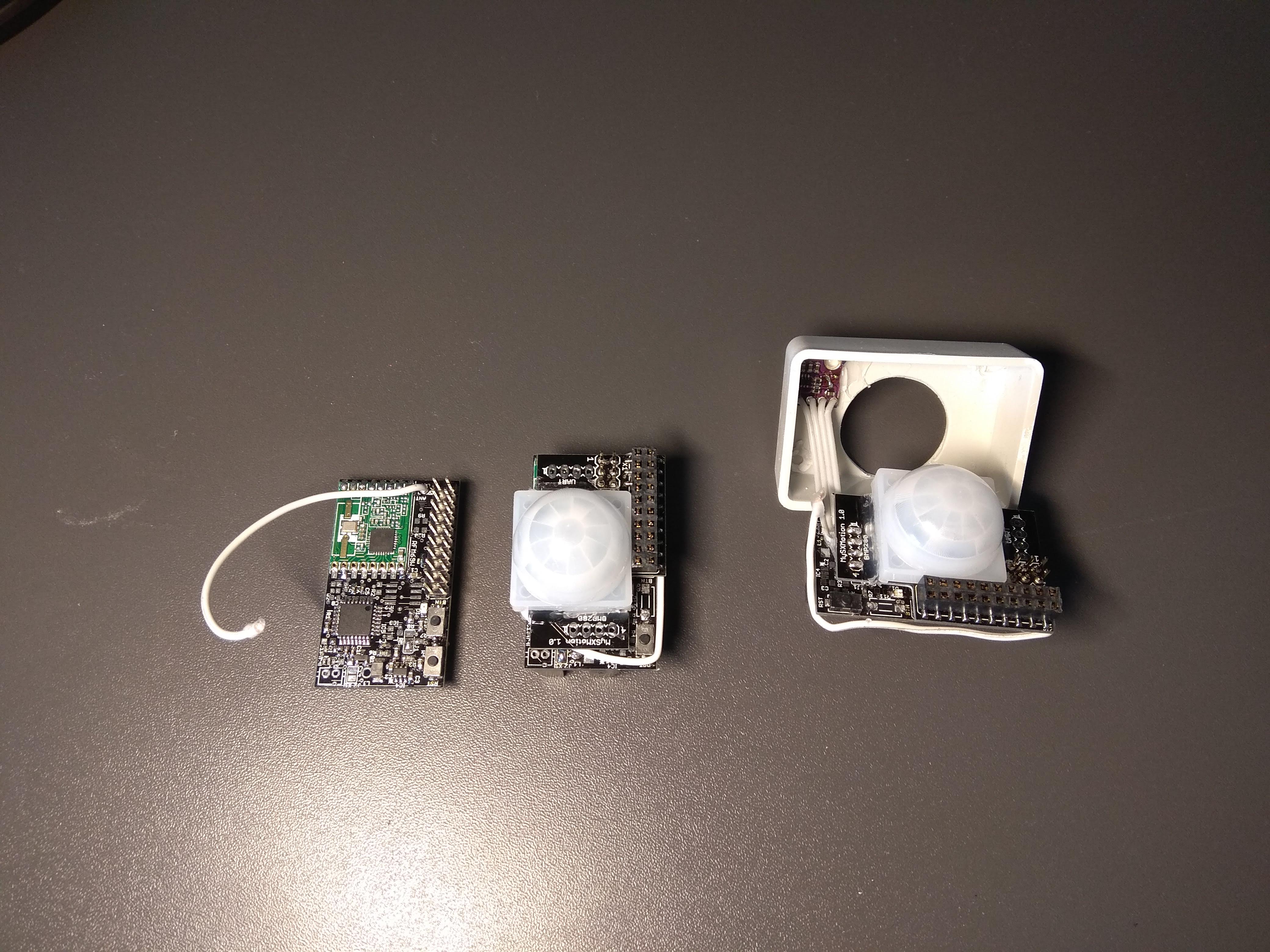
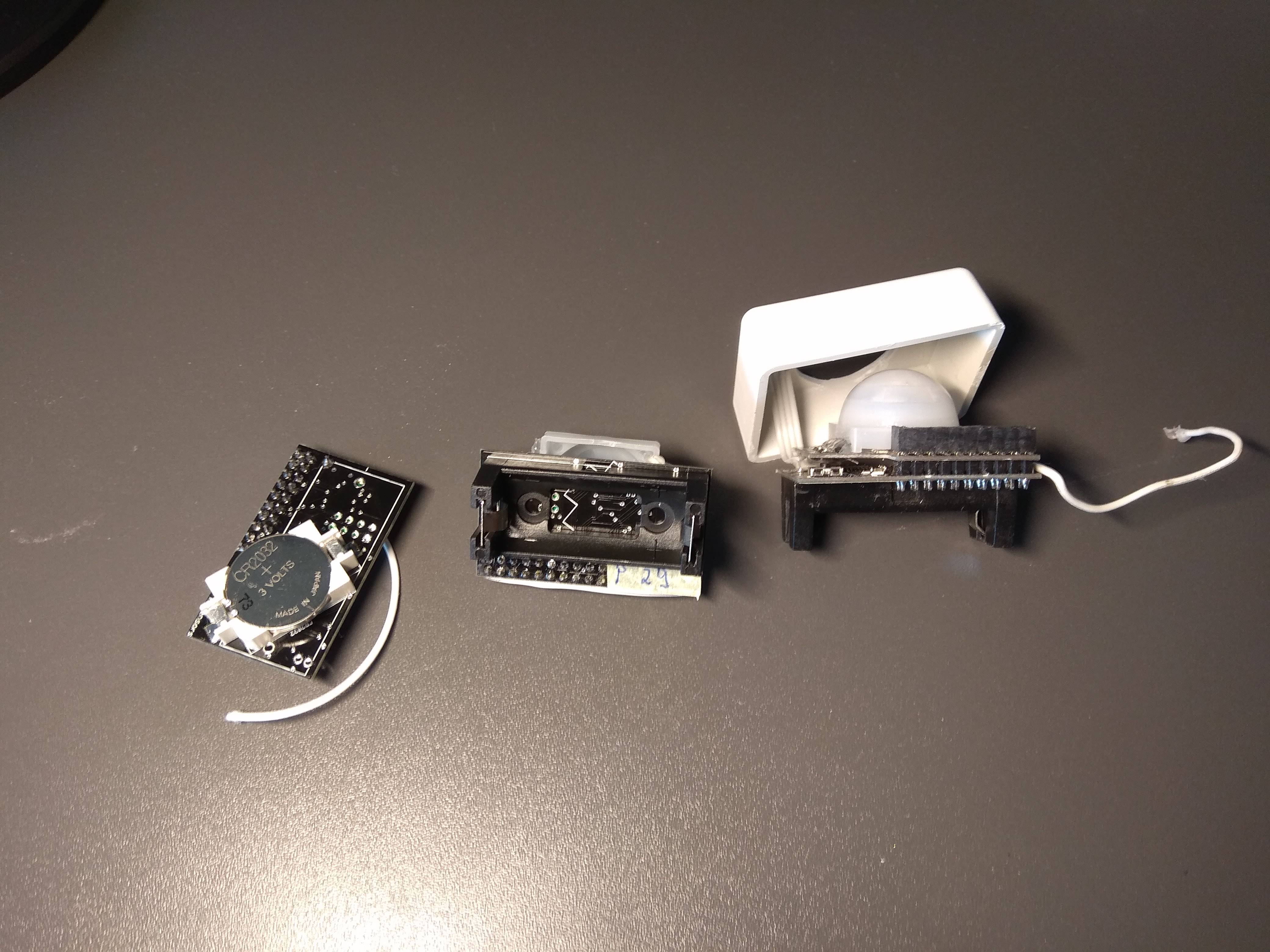
This is a motherboard for creating MySensors nodes based on the atmega328p MCU. It is meant to be combined with a MySX daughter board to create fully functional MySensors node. It is primarly for battery powered nodes but can be also used as a gateway or ac powered node (ac power supply is not part of this project). It features multiple powering options and supports both NRF24 and RFM69 RF modules. The size of the board is just a little bigger than a cr123a battery holder.


Features:
- atmega328p MCU
- Multiple power source options:
- CR123A battery or 16340 rechargable li-ion battery
- CR2032 battery
- JST-PH2 connector for rechargable li-ion battery
- VRAW from MySX connector
- Multiple voltage regulator options:
- MCP1640C boost converter with bypass option
- TPS782 LDO linear regulator
- no voltage regulation - direct voltage from battery
- Battery reverse polarity protection
- Battery voltage divider to monitor battery voltage
- ATSHA204A supported
- AT25DF512C flash suppoerted
- NRF24L01 RF THT module
- RFM69 RF SMD module
- RF module interrupt D2 pin can be disconnected if not used
- reset button
- user button
- user led
- external oscillator for atmega
HOW TO
Minimum required parts to solder are:
- MCU related parts: C5, C6, C7, C10, IC5, R7
- Radio module related parts: C1, R1
- for NFR24 option solder NRF24L01
- for RFM69 option solder RFM69W, antenna to ANT pad and R12 (R12 is just a 0Ohm jumper required to connect RFM69 interrupt with D2 pin)
- MySX connector: X2
This is bare minimum that is required to start with this board. In this configuration the board can be powered from the MySX connector VCC pin with voltage between 1.9V - 3.6V.
Optional parts to solder are:
- MCU related parts:
- for user led - R8, D1
- for reset button - RST
- for user button connected to D2 pin - BTN
- for I2C pull-up resistors - R9, R10
- for external oscillator - C8, C9, Q2
- External flash related parts: R2, IC2 WARNING: flash chips consumes a lot of uA of current so it is not suited for battery powered nodes.
- ATSHA204A related parts: IC3 ATSHA204A requires at least 2.0V power supply
Powering options
The powering option is choosed in two steps. First is to select the voltage source, and second is to choose the voltage conversion type. Between the voltage source and the voltage converter ther is the reverse battery protection mosfet Q1 which is required for all options and voltage divider for battery voltage monitoring which is not required.
Voltage source options are:
- CR123A battery or 16340 rechargable li-ion battery. To select this option just solder CR123A battery holder.
- CR2032 battery. To chosse this option just solder CR2032 battery holder.
- JST-PH2 connector. To choose this option just solder the X1 connector.
- VRAW from MySX connector. To choose this option the J2 jumper must be shorted.
Reverse polarity battery protection: Q1
Voltage divider for battery voltage monitoring: R5, R6, C4
Voltage convertion options are:
- MCP1640C boost converter R3, R4, R11, C2, C3, L1, IC4, J1 jumper should connect VBOOST with VCC. The MCP1640C boost converter can be put into bypass mode so it just passes the input voltage. It is controller by the A2 pin and the bypass mode is the default. The purpose of this functionality is to be able to run the MCU directly from the battery and to boost the voltage only for the moment required to make measurements with sensors that require higher voltages.
- TPS782 LDO linear regulator C13, C14, IC1. J1 jumper should connect VREG with VCC. The C12 should be replaced by the 0Ohm resistor. The C12 capacitor was designed for the APE8865 LDo which consumes much more current that TPS782.
- No voltage regulation There is actually no direct way to shoose this option, but it can be done by shorting pins number 5 and 6 of the IC4 and J1 jumper should connect VBOOST with VCC.
Powering examples.
Very low power temperature and humidity sensor based on the BME280 sensor. This node uses the "No voltage conversion" option because the BME280 sensor can work with voltages as low as 1.2V. So the node may be powered just by 3V coin-cell battery. This type of node uses just CR2032 battery holder.
Very low power node with DS18B20 temperature sensors that require minimum 3V power supply. This type of node uses MCP1640C boost converter to boost battery voltage for the measurement period. Use CR2032 battery holder and MCP1640C boost converter option. In the software controll properly the A2 pin to turn on/off boost conversion.
Motion sensor node. Motion sensor such as AS312 consumes quite a lot of power and needs voltage between 2.7V and 3.3V. Powering it directly with 3V battery is not good, so we could use the boost converter. But boost converter makes to much noise for AS312 to work properly. The AS312 works the best with 3V LDO, so the power source should have higher voltage. The best options is to use 3.7V 16340 rechargable li-ion battery which fits into CR123A battery holder. Use TPS782 LDO option to power the MCU and RF module and short the J2 jumper to power the VRAW pin directly with 3.7V battery. Then the motion sensor daugher board should power the AS312 sensor with another LDO from the VRAW pin.
